Bolt:A Stateful Processor Interconnect
Abstract
The wireless sensor network community is currently under-going a platform paradigm shift, moving away from classical single-processor motes toward heterogeneous multi-processor architectures. These emerging platforms promise efficient concurrent processing with energy-proportional system performance. The use of shared interconnects and shared memory for inter-processor communication, however, causes interference in the time, power, and clock domains, which pre- vents designers from fully harnessing these benefits. We thus designed Bolt, the first ultra-low-power processor interconnect for the compositional construction of heterogeneous wireless embedded platforms. This paper presents the architectural blueprint for interconnecting two independent processors, while enabling asynchronous inter-processor communication with predictable run-time behavior. We detail a prototype implementation of Bolt, and apply formal methods to analytically derive bounds on the execution time of its message passing operations. Experiments with a custombuilt dual-processor platform show that our Bolt prototype incurs a negligible power overhead relative to state-of-the-art platforms, offers predictable message passing with empirical bounds that match the analytical ones to within a few clock cycles, and achieves a high throughput of up to 3.3 Mbps.
Main content
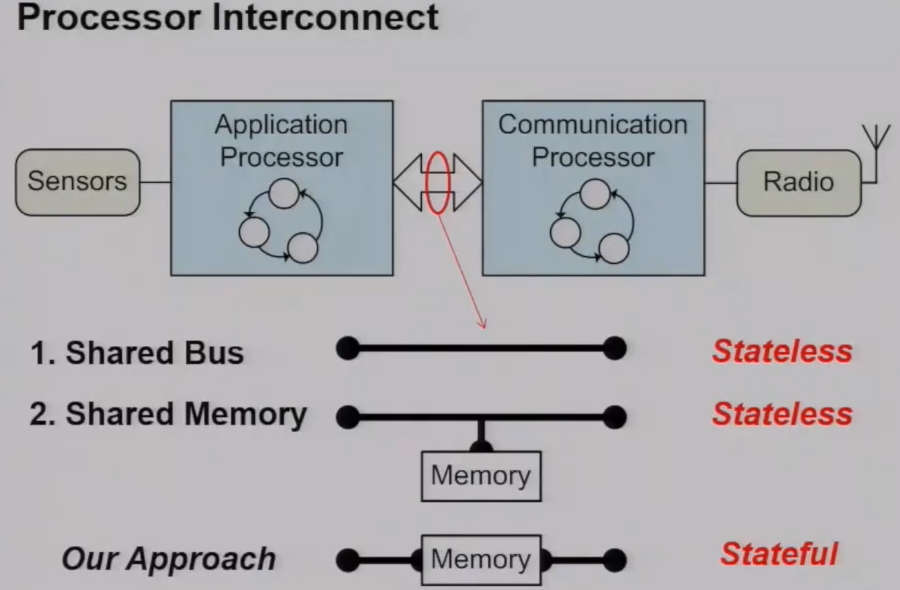
Low-power operation was achieved by interleaving sensing, data processing, and communication tasks and by judiciously managing the power state of hardware components. The engineering effort in realizing such systems is labor-intensive with respect to the design, test, and diagnosis of hardware and software components. While difficult to quantify, so these practical complexities lead to implementations that are often unreliable, not readily adaptable to changing requirements, exhibit long development cycles, and are over-dimensioned to satisfy performance targets. Why is it difficult to design such systems? The main problem is rooted in the interference of hardware and software components in the time, power, and clock domains. Reading sensors, processing data and transmitting packets is executed concurrently. These concurrent tasks interfere when they compete for shared resources such as clock cycles, memory, and peripherals. Although some measures may be effective in a short period of time, it will have a very bad impact on the system for a long time and will also affect the operation. This paper presents Bolt, the first processor interconnect that enables the composable construction of ultra-low-power wireless embedded systems.Bolt provides predictable asynchronous communication between two arbitrary processors, and thus decouples the processors in the time, power, and clock domains. let’s look at the main techniques that are used to interconnect these two cores. The first of which is a shared bus. It’s a stateless interface meaning that the state of the infirm state of the bus is managed by both application and communication processor and this shared bus links these two cores in time power and clock domains. To give an example if the application processor wants to send a message to the communication processor. Communication processor must stop what it’s currently executing in order to receive the message and process it. Therefore linking the two cores in the time domain. If the communication process however was in a deep sleep mode, it would actually have to be forced to wake up into an active mode in order to receive this message and process it. There by linking the two cores in the power domain. Furthermore these two cores would also have to agree in advance on a clock frequency. In order to share messages across the shared bus there by linking them in the clock domain. A popular alternative is to use shared memory and essentially a shared bus with some memory that’s addressable by both cores. While because we also have a shared bus, we still link these two cores in time, power and clock domains while it also is a stateless bus. The stateless interconnect since the application and communication processor must manage the software structures that enable message transfer between the two cores. Our approach is a stateful processor interconnect, whereby we use dedicated bus which interfaces to an intelligent memory interface or memory block.
We call this memory block bold a stateful processor interconnect and were able to decouple these two processes in the power and clock domains using asynchronous message passing between the two cores. What’s more important or even more important is that we’re able to perform this asynchronous message passing with predictable timing properties. Now bolt is a combination of hardware and software but sits in between these two arbitrary processes a consisting of a message controller and which manages to fifo queues for one for each flow one for each message flow. And these message queues reside in non-volatile memory. So we’re able to decouple these two these two processes in the time and power domains since each process is free to read and write messages according to its local execution policy and similarly they’re able to operate in their own clock domains. Since they have dedicated control and data buses.
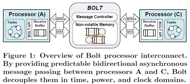
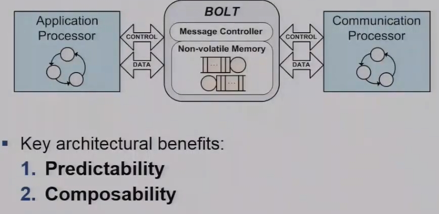
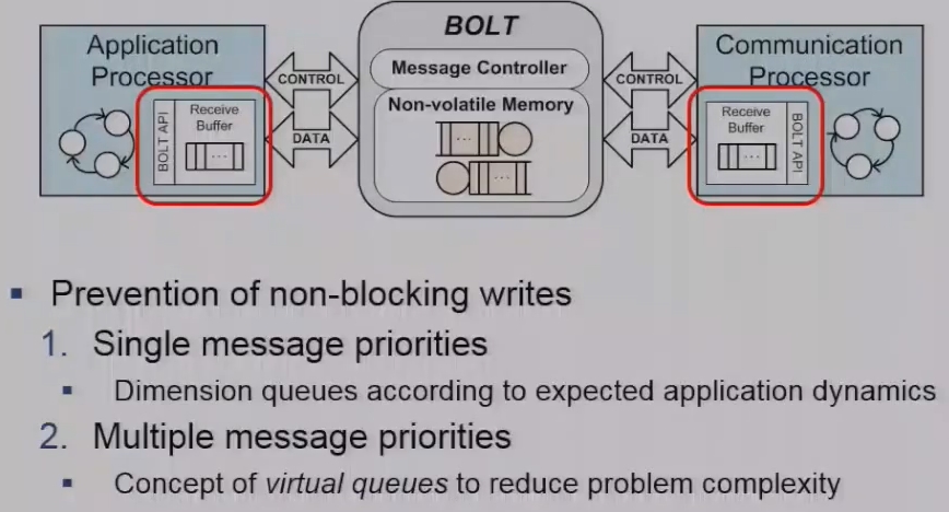
As depicted in Fig. 1, Bolt is a piece of integrated hardware and software that sits between two processors A and C. Bolt lets A and C asynchronously exchange messages while executing within their own time, power, and clock domains. Bolt adopts asynchronous message passing to avoid interference between processors A and C wherever possible.


Avoid resource interference
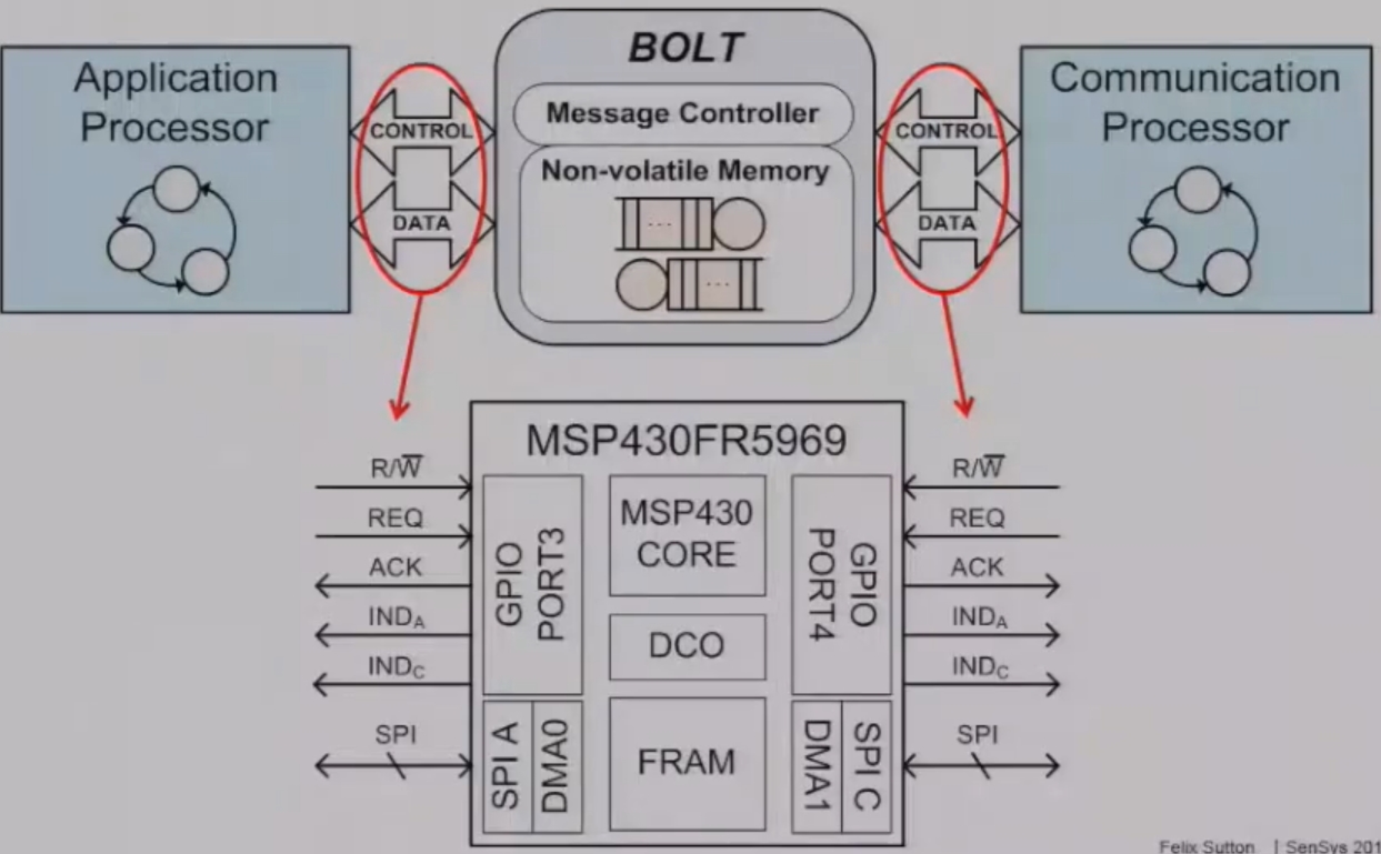
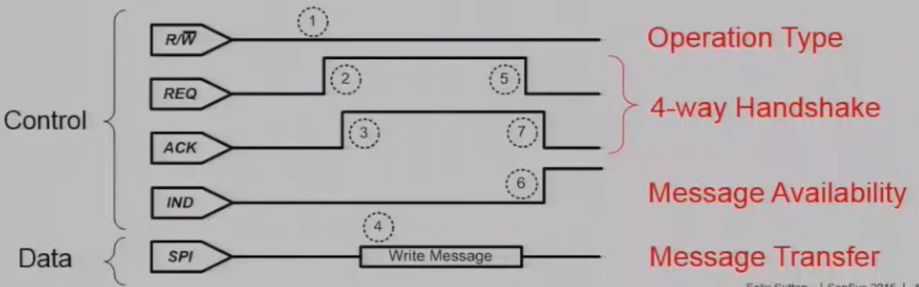
The author firstly avoid resource interference by allowing messages to be performed on a control and data interface which are dedicated to each processor. More importantly, it map these control and data paths on two independent Hardware blocks within microcontroller. So it used independent GPIO ports, independent SPI and DMA to provide the message transfer. Firstly using a single GPIO pin to define the type of message that will type of operation whether it be read or write. Then using a request in an acknowledgement pin to provide a 4-way handshake for a processor to request control over the SPI data transfer. Lastly an indication pin that provides information to the processor that at least one message is available to read out. The data path is implemented using standard three wire SPI bus with the important factors that bolt is always the SPI slave allowing each of the processes to drive the clock of the SPI bus. So now it has avoided the resource interference wherever possible.
If unavoidable, tightly bound resource interference
we now seek to tightly bound any unavoidable resource interference and indeed we have unavoidable resource interference particularly when we have simultaneous message operations. An example illustrated here when the application processor writes a message in while the communication processes simultaneously reads a message out of this FIFO queue we encounter resource interference on our bolt implementation both in terms of software and in terms of hardware.
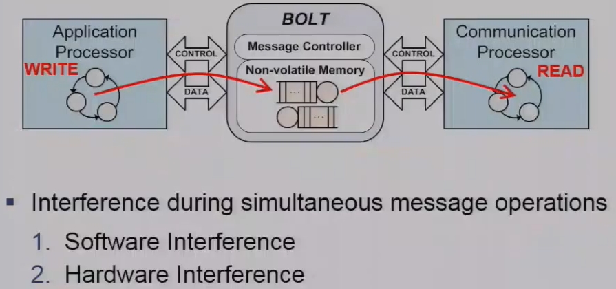
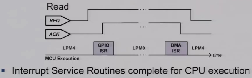
we’ll look at these two cases individually. The bolt software state machine is purely interrupt driven and this figure illustrates the microcontrollers execution over time with respect to the message operation which is driven by the four-way handshake. During no operation or when there’s no message to transfer our microcontroller is in deep sleep or LPM4 mode for and when during the four-way handshake. This triggers an external interrupt on a microcontroller, we perform the necessary setup of the internal peripherals and memory using a GPIO interrupt service routine. During the actual message transfer, the microcontroller resides in LPM0 mode while the DMA’s are active. Then lastly the handshake completes the message transfer again triggering a GPIO is our before the microcontroller returns to a deep sleep mode.
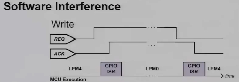
Similarly a read operation is very similar with the difference being that a DMA what’s triggered to the commit phase of a read operation. As we can see if we will perform write and read operation simultaneously, these interrupt service routine will compete for CPU execution essentially causing resource interference on a microcontroller.
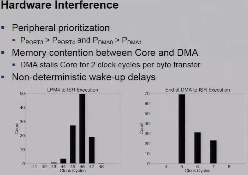
A second aspect is Hardware interference that we see on BOLD. This is primarily due to three independent reasons. The first one is that the microcontroller imposes a fixed priority scheme for all interrupts. So we see that the port interrupts for three and four on the GPIO port where PORT3 is has higher priority than PORT4. Similarly the DMA channels also have DMA0 has a higher priority then the DMA1. So when interrupts occur simultaneously, clearly one is it will be executed in front of in preference of the other. Also we perform or data transfer is handled using DMA towards from the SPI modules to the internal frame. And the DMA stores stalls the MCU for precisely two clock cycles per byte transfer. So this also has to be factored into when we want to evaluate or determine type worst-case execution times of read and write operations. Lastly we have non-deterministic wake up delays on a microcontroller. so contrary to what most data sheets provide will specify the wakeup times between. for example LPM4 is our execution or indeed the end of an DMA operation actually have a very highly non-deterministic execution time and these are two examples where we characterize these delays using a logic analyzer on our prototype.
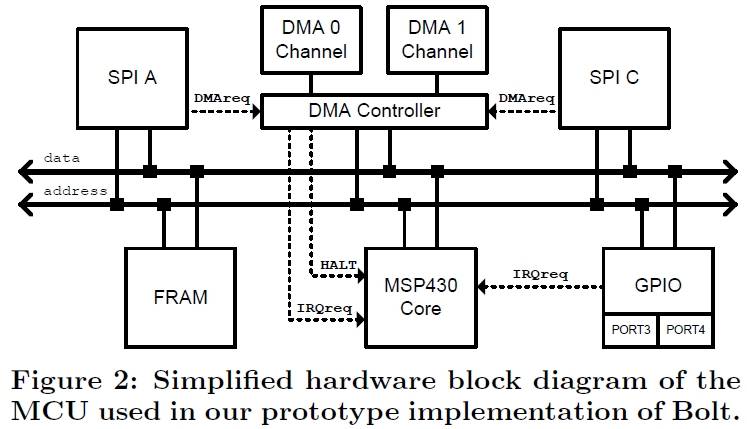
So we need to factor not only the software interference but also the hardware interference in order to define the worst-case execution time for our read and write operations. In order to do this, we use or apply a formal method. so we first constructed a model of the msp430 cpu using information available in data sheets that user guides etc. here we see the GPIO block for the 4-way handshake and the SPI and DMA channels are handled by DMA controller internal FRAM and the msp430 core.
so we mapped this model into loophole which is a very popular and very widely used a timed automated model checker and were able to construct what ended up being quite a complex model consisting of more than or nine automaton where we modeled each of the hardware and software interactions going on within bolt it consisted of more than 120 states more than 160 transitions.
Specify an interface with formally verified properties
BOLT IMPLEMENTATION
Hardware Architecture
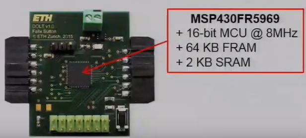
The author implement a Bolt prototype using the 16-bit TI MSP430FR5969 MCU running at an 8MHz clock frequency. The core, the FRAM, and all peripherals are attached to a shared 16-bit data bus and a 20-bit address bus. The instruction processing of the core may be interrupted by either the generalpurpose input/output (GPIO) module or the direct memory access (DMA) controller using auto-vectored interrupt processing.
The GPIO module has two ports, namely PORT3 and PORT4. PORT3 has a higher priority than PORT4. The MCU provides two independent SPI hardware modules, namely SPI A and SPI C. The byte-wise transfer be- tween the SPI receive buffer and the FRAM is coordinated by dedicated DMA channels, that is, DMA0 for SPI A and DMA1 for SPI C. The DMA controller manages the bus arbi- tration and interrupt priority, with DMA0 having a higher priority than DMA1. Allow the CPU to run the current cycle before the DMA starts. The byte transfer between SPI and FRAM takes precisely two clock cycles.A dedicated GPIO port is used to implement the control channel toward each interconnected processor. PORT3 is assigned to processor A, while PORT4 is assigned to processor C.
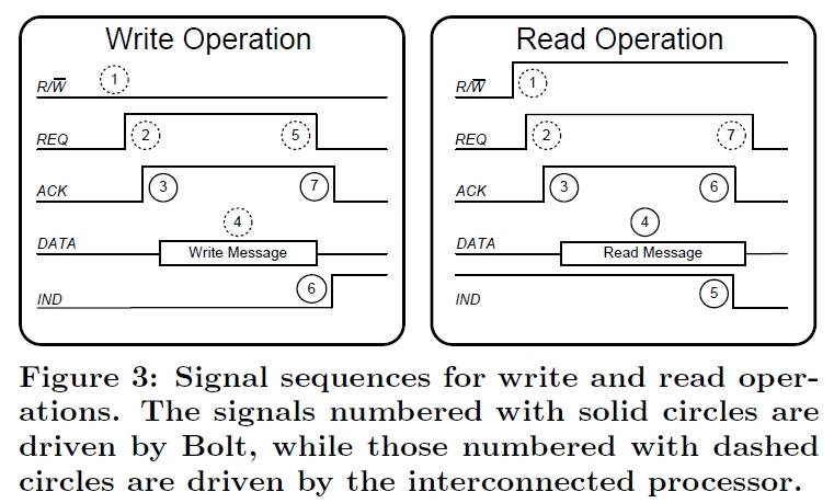
The control channel consists of the four lines R/W, REQ, ACK, and IND. The R/W line defines the requested operation as either a message read or a mes- sage write. The REQ line is used by the interconnected pro- cessor to request the specified message operation, while the ACK line is used by Bolt to grant a message transfer over the corresponding data channel. The two REQ lines are configured as interrupt wakeup sources. The MCU is put into deep sleep (LPM4), while all other hardware blocks are turned off. The MCU remains in deep sleep until a read or write operation is initiated.
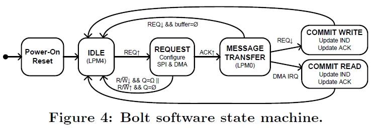
When either processor initiates a read or write operation by setting the R/W line and raising the REQ line, the associated IRQ wakes the MCU from deep sleep. Once the core is awake, the GPIO ISR will first determine the requested mode of operation and configure the corresponding SPI module and DMA channel for message transfer before updating the ACK line accordingly. The MCU will then enter a low-power mode (LPM0) with the core turned off, while the DMA and SPI modules remain active.
The completion of a message transfer is also processed by an ISR. However, depending on the message operation, either the GPIO or DMA ISR will be invoked. If the operation is a write, the falling edge of the REQ line signals the end of the message, thereby invoking the GPIO ISR. If the operation is a read, the DMA controller will trigger an interrupt toward the core. The ISR will update the internal data structures, update the ACK and IND lines, and disable the associated SPI and DMA peripherals. If there is an on-going message transfer involving the alternate processor, the MCU will return to the LPM0 sleep mode; otherwise it will return to the LPM4 deep sleep mode.
If interference is unavoidable, try to tightly bound it. An approach, and one that has been well-studied in the embedded systems community, is to use formal methods such as model checking. Through the construction of an accurate model of the system, one can apply rigorous mathematical tools to analytically derive safe bounds on interfering resources. The challenge in constructing a model of our Bolt prototype is capturing the complexity of several time-dependent and interacting state machines each of which has their own independent clock domain. As a solution to this challenge we propose to model all interactions as timed automata and to extend each automaton with an independent clock variable.

Fig. 10 shows a custom-built heterogeneous dual-processor platform, where Bolt interconnects two state-of-the-art processors with different computing capabilities and power dissipation: a 32-bit STM ARM Cortex-M4 STM32F303VCT6 running at 72 MHz and a 16-bit TI CC430F5137 SoC running at 20 MHz.
When Bolt does not perform reads or writes, its power dissipation of 1.3 µW is less than state-of-the-art low-dropout voltage regulators. Bolt’s active power dissipation of 1.1 mW is comparable to the sleep mode power dissipation of the Cortex-M4.
Paper
Paper 👉Paper Pages
Video 👉Video
Github 👉Github
ETH 👉ETH